


Description
The TBMDA-BCI25 modulated amplifier provides the necessary bandwidth and modulation for conducted immunity testing using BCI probes per ISO 11452-4 in the frequency range from 1 MHz to 400 MHz. It is designed to be driven by signal generators or by tracking generators of spectrum analyzers. With a 1 dB compression point of up to 30 W in the frequency range 1 MHz to 400 MHz it can generate test levels up to 400mA. A built in AM / PM – modulator enables use of tracking generators as signal source. The TBMDA-BCI25 has sufficient gain to achieve maximum output power with 0 dBm provided by a spectrum analyzer tracking generator.
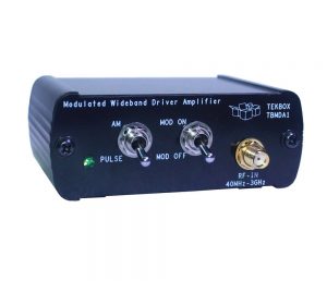
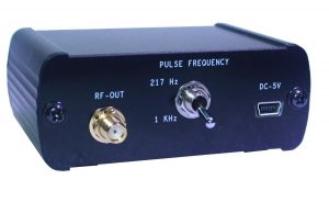
Besides 1 kHz, 80% AM, the TBMDA-BCI25 provides built in modulation capability to generate 1 kHz, 50% duty cycle PM signals. In PM mode, the TBMDA-BCI25 can also generate a 217 Hz Signal with 12.5% duty cycle in order to simulate mobile phone TDMA noise.
FEATURES
- CW amplifier (modulation off)
- 1 kHz, 80% AM modulation
- 1 kHz, 50% duty cycle pulse modulation
- 217 Hz, 12.5% duty cycle pulse modulation
SPECIFICATIONS
- Input / Output: 50 Ohm, N female
- Supply Voltage range: 110 V…240 V
- Supply power consumption: 108 W @ 220V
- Operating temperature range: -20°C to 50°C
- Frequency range: 1 MHz – 400 MHz
- Small signal gain: 47 dB typ.
- Gain flatness 1 MHz – 400 MHz / Pin = -3 dBm: 1.5 dB typ.
- Saturated output power @ 1 MHz / Pin = 0 dBm: 45.1 dBm (32.2 W) typ.
- Saturated output power @ 10 MHz / Pin = 0 dBm: 45.2 dBm (33 W) typ.
- Saturated output power @ 50 MHz / Pin = 0 dBm: 45.9 dBm (38.6 W) typ.
- Saturated output power @ 100 MHz / Pin = 0 dBm: 45.7 dBm (37.5 W) typ.
- Saturated output power @ 150 MHz / Pin = 0 dBm: 46.2 dBm (41.2 W) typ.
- Saturated output power @ 200 MHz / Pin = 0 dBm: 45.6 dBm (36.1 W) typ.
- Saturated output power @ 250 MHz / Pin = 0 dBm: 46.3 dBm (42.5 W) typ.
- Saturated output power @ 300 MHz / Pin = 0 dBm: 46 dBm (39.7 W) typ.
- Saturated output power @ 350 MHz / Pin = 0 dBm: 45.8 dBm (37.8 W) typ.
- Saturated output power @ 400 MHz / Pin = 0 dBm: 45 dBm (31.6 W) typ.
- 1dB output compression point @ 1 MHz: 44.1 dBm typ. (Pin: -4 dBm)
- 1dB output compression point @ 10 MHz: 44.6 dBm typ. (Pin: -3 dBm)
- 1dB output compression point @ 50 MHz: 45.3 dBm typ. (Pin: -2 dBm)
- 1dB output compression point @ 100 MHz: 45.2 dBm typ. (Pin: -1 dBm)
- 1dB output compression point @ 150 MHz: 45.2 dBm typ. (Pin: -2 dBm)
- 1dB output compression point @ 200 MHz: 45.2 dBm typ. (Pin: -1 dBm)
- 1dB output compression point @ 250 MHz: 45.6 dBm typ. (Pin: -2 dBm)
- 1dB output compression point @ 300 MHz: 45.1 dBm typ. (Pin: -2 dBm)
- 1dB output compression point @ 350 MHz: 44.8 dBm typ. (Pin: -2 dBm)
- 1dB output compression point @ 400 MHz: 43.6 dBm typ. (Pin: -4 dBm)
- 2 nd harmonic, 100 MHz, Pout = 45.7 dBm: < – 23 dBc typ.
- 2 nd harmonic, 100 MHz, Pout = 40 dBm: < – 29 dBc typ.
- 3 rd harmonic, 100 MHz, Pout = 45.7 dBm: < – 12 dBc typ.
- 3 rd harmonic, 100 MHz, Pout = 40 dBm: < – 19 dBc typ.
TOTAL HARMONIC DISTORTION
- 8.6% @100MHz, Pout = 37 dBm typ.
- 12.1% @100 MHz, Pout = 40 dBm typ.
- 17.6% @100 MHz, Pout = 43 dBm typ.
- 25% @100 MHz, Pout = 45.7 dBm typ.
- Third order output intercept point: 49 dBm, @100 MHz, ∆ f = 2MHz, typ.
- Internal modulation frequency AM: 1 kHz ±20%
- Internal modulation frequencies PM: 1 kHz ±20%, 217 Hz ±20%
- Duty cycle, PM: 50% ±10% @ 1 kHz; 12.5% ±20% @ 217 Hz
MAXIMUM RATINGS
Maximum input power: +0 dBm
The output of the TBMDA-BCI25 is quite tolerant to output mismatch, however open or shorted load is not recommended, as it potentially can cause damage to the output transistor. When driving near field probes, current probes or any load of unknown impedance, it is highly recommended to insert a ≥ 3dB attenuator at the output of the amplifier in order to protect the output stage.
APPLICATION
- General-purpose wideband RF power amplifier
- Wideband RF power amplifier for conducted immunity testing driving BCI-probes
- Wideband RF power amplifier for radiated immunity testing, driving near field probes
- Wideband RF power amplifier for radiated immunity testing, driving TEM Cells

Reviews
There are no reviews yet.